

TPC Readout 2000
CERES
2000/2001
1 Front-End-Electronic
For the beam-time in 2000 the readout system of the TPC was completely changed. Instead of using a 16-bit digital data link between the front-end electronics and the motherboards, on which the data were compacted and reformatted, an analog connection to the FEDC-boards1 was used. Because the output of the SCA was not able to drive this long line (about 14 m), an external line driver (linear buffer) was used. This driver was realized on a small PCB which was glued directly to the FEE-boards. In the new setup the motherboards were only used for configuring the front-end electronics and for distributing the trigger/abort signals.
2 The FEDC-board
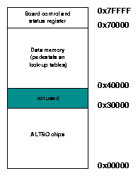
The digitization and further processing of the TPC signals is done on the FEDC-boards. These boards are realized as a 9U VXI device which can contain up to 48 readout channels. Each readout channel comprises a 10-bit ADC and a digital ALTRO2 chip. Four ADCs together with four ALTROs are arranged on one daughter card. For the CERES readout only 40 channels were used. Some global control registers and memory for the processed data completes the board. The FEDC-board is an A32 slave. The 5 MSB, A31-A27, define the board address. The remaining 19 bits (A18-A0) define the FEDC's address space which is shown in Figure 1.
|
|
The behavior of the ALTRO chip is controlled by a set of internal control/status registers. Table 1 shows the function of these registers together with their addresses.
| Address | Name | Access | Description | |
| 0x70000 | CSR0 | R/W | [31:0]: | enable bit for channels 0 to 31 |
| 0x72000 | CSR1 | R/W | [15:0]: | enable bit for channels 32 to 47 |
| 0x74000 | CSR2 | R/W | [19:16]: | trigger delay |
| [12:0]: | readout delay | |||
| 0x76000 | CSR3 | R/W | [31]: | flag |
| [30:21]: | event number | |||
| [20:16]: | board address | |||
| [15:0]: | event length | |||
| 0x7a000 | RST | W | RESET | |
| 0x7b000 | EVRST | W | event counter RESET | |
| 0x7c000 | TRG | W | trigger | |
The control and status registers of the ALTRO chip are shown in table 2.
| Address | Name | Access | Description | |
| 0x800 | CSR0 | R/W | [16:9]: | number of samples to process |
| [8:1]: | zero suppression threshold | |||
| [0]: | data stream coming from ADC (=0) or pedestal memory (=1) | |||
| 0xa00 | WBASL | R | access to pedestal memory | |
2.1 Signal Processing
Immediately after receiving a trigger signal the SCA starts to sample the 16 outputs of the amplifier in parallel. These sampling phase is followed by the readout phase in which the stored analog values are dumped in a time-wise order (first sample of channel 0, fist sample of channel 1, Œ, fist sample of channel 15, second sample of channel 0, Œ).During the readout phase the output signal of the SCA has a maximum swing (AC component) of 2 V and baseline (DC component) that can be adjusted online via a DAC on the FEE-board. In the linear buffer (on the FEE-board) the signal is shifted and compressed in order to match the FEDC dynamic range. For the baseline at the output of the SCA a value of -0.5 V (used in the '99 run) is assumed.
The data coming from the TPC front-end electronic is digitized using a 10 bit ADC. After converting the analog signal the data stream is demultiplexed according to the 16 channels of the preamplifier. The resulting 16 data streams are processed in parallel inside the ALTRO chip. Inside the ALTRO chip the data is represented and processed only with the 9 MSB, resulting in a loss of 1 bit in resolution. Therefore, in the ALTRO chip the signal is described by a 9 bit code (0 - 511) with a baseline at about 300.
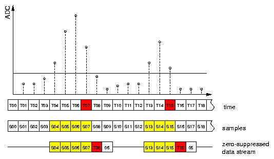
In the following processing steps the polarity of the signal is changed and the baseline is subtracted. After this subtraction the signal should be contained in the first half of the 9 bit range. Therefore the most significant bit can be omitted reducing the signal representation to 8 bit codes. Finally the signal undergoes the zero suppression. Samples with a value smaller than a constant threshold (8 bit) are rejected. When a sample is found to be above the threshold, it is considered as the start of a pulse.
|
|
2.2 Data format
32bit words!!256 bytes/event/ALTRO -> 250 bytes of data
The FEDC event is stored in memory as a back-linked structure. Due to the removal of a various number of samples between accepted clusters, the timing information would be lost during the zero-suppression process. This requires the addition of two additional words - the time-stamp and the cluster-length. The cluster-length corresponds to the total number of samples plus the time-stamp and the cluster-length. The time-stamp gives the (sample-)position of the last sample in the cluster relative to the trigger signal. This cluster structure (sample values + time-stamp + cluster-length) is repeated for each accepted cluster in a specific channel.
| sample 0/3 | sample 0/2 | sample 0/1 | sample 0/0 |
| sample 1/0 | length 0 | time 0 | sample 0/4 |
| time 1 | length 1 | sample 1/2 | sample 1/1 |
| sample n/3 | sample n/2 | sample n/1 | sample n/0 |
| XX | XX | length n | time n |
| block length | channel id | ||
The overall FEDC-board data block contains the channel data blocks, one after the other, from channel 0 to channel 703. In the CERES version, the FEDC-board uses only 640 of the 768 available channels, numbered from 0 to 319 and from 384 to 703. The FEDC
2.3 Pedestals
Because each ALTRO chip process data coming from 16 TPC-channels with maximum 256 time samples (= 4096 bytes), it was not possible to provide enough memory inside the chips to hold pedestal values for all samples. Instead, a scheme using a look-up table was implemented. Figure 3 shows a pictorially representation.
|
|
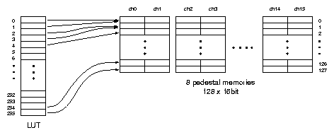
The look-up table contains 256 7 bit words. The index (the linenumber) of this table corresponds to the sample number. The entries are the addresses of the data-buffers which contain the pedestal values. This means, 128 pedestal values can be assigned to each channel. For this scheme only 2048 bytes for the data plus 256 bytes for the look-up table are necessary.
The format of the data files used to program the pedestal values reflect this setup. The information belonging to 4 ALTROS of one daughter card are combined in one file. The file name contains the branch number (x), the FEDC-board number (y) and the daughter card number (z): ped_x_y_z. Each ALTRO data block consists of the pedestal values and the look-up table. The pedestal values are arranged in 128 lines with eight 16 bit words. The first word contains the information for channel 0 and 1, the second for channel 2 and 3, and so on. The look-up table, which follows the data block, consists of 256 lines each line containing a 7 bit word.
3 The MXI-2 Interface
The MXI-bus3 is a high-performance communication link that interconnects devices using a flexible cabling scheme. MXI-bus is a general purpose, 32-bit multi-master system bus on a cable. It provides a high-performance way of controlling VXI4 systems using commercially available desktop computers and workstations. MXI devices can directly access each other's resources by performing simple read and write operations to appropriate address locations. The MXI-2 standard expands the number of signals on a standard MXI cable by exporting all VXI backplane signals such as VXI triggers, interrupt lines and system clocks directly to the cabled bus.A VXI device has a unique logical 8-bit address, which serves as a means of referencing the device in the VXI system and allows up to 256 VXI devices in a VXI system. Each VXI device must have a specific set of registers, called configuration registers. These registers are located in the upper 16 kB of the 64 kB A 16 VME address space. The logical address of a VXI device determines the location of the device's configuration registers in the 16 kB area reserved by VXI.
Through the use of the VXI configuration registers the system can identify each VXI device, its type, model and manufacturer, address space, and memory requirements. VXIbus devices with only this minimum level of capability are called register-based devices. With this common set of configuration registers, the centralized Resource Manager, a software module, can perform automatic system configuration when the system is initialized.
In addition to register-based devices, the VXIbus specification also defines message-based devices, which are required to have communication registers in addition to configuration registers. All message-based VXIbus devices, regardless of the manufacturer, can communicate at a minimum level using the VXI-specified Word Serial Protocol. In addition, one can establish higher-performance communication channels, such as shared-memory channels, to take advantage of the VXIbus bandwidth capabilities.
The setup used in CERES consists of the VME FEDC-boards which are controlled by an PCI-VME bridge - the National Instruments VME-MXI-2 bus extender. This configuration consists of a PCI card (plugged in the so called Readout-PCs), MXI-2 bus and a MXI-VME interface card. Data and control signals are converted on the PCI board and sent over the MXI bus, which is essentially the VME on a cable, into the MXI-VME interface board. The 6U MXI-VME interface board in conjunction with the MXI-2 cable enables data transfers up to 38 MBytes/s using D64 transfers.
4 Software
4.1 The OS9-System
|
|
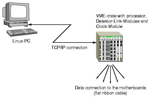
The communication with the TPC-electronic is based on a VME processor running the OS9 operating system (FIC 8234 from CES). For the 2000 run the software philosophy was changed and the user-programs adapted to Linux. The communication between user and hardware rely an a very simple client/server architecture. The programs, started on a PC running Linux, open a TCP/IP connection to the VME processor and send short commands to it which initiate a VME-bus access. In case of a read access the data are sent back to the PC using the established TCP/IP connection. The server software on the OS9 system is called vme_server.c . This concept worked very reliable. The main disadvantage of this system was a slower program execution speed.
Some of the following programs (especially those which process raw data) can only be executed on a PC with a ramdisk (or a directory) at /dev/ramdisk. The PC which was used during the 2000 run was pcceres37.
4.2 Library
- TPClib_new.c
- This library is used by every user program. It contains routines for the communication with the OS9-system as well as data structures representing the hardware setup of the TPC electronic.
4.3 TPC Control
(xx = chamber number)- TPCclock
-
Program to set the "Masterclock" for the TPC-readout.
Usage: TPCclock <clk> clk: clock value in MHz - TPCinit
-
Program to initialize the TPC according to the setup files.
Usage: TPCinit <trials> trials: number of trials to init FEE Files: TPCsetup.sc tpc_xx_md.asc - TPCon
-
Program to switch on the power for the TPC according to the setup
files.
Files: tpc_xx_ON - TPCoff
- Switch off the FEE-boards.
- TPCedit
- Simple text based editor for modifying the
power settings of the FEE-boards. The program enables the switching of
a single board or of a group of boards.
Files: tpc_xx_ON - TPCabort
- Sends a software abort to the Clock-module which distributes it to the motherboards.
4.4 Pedestal Software
- TPCpedestals
-
This program calculates the pedestals and writes them in the proper
format in files which can be used for the programming of the
FEDC-boards. The input data are read from the ram-disk. The output
files are written into the Pedestal_calc directory.
Usage: TPCpedestals <sigma> <mask> sigma: number of sigma added to the threshold mask: 1: acceptance mask for normal B-field 0: no acceptance mask -1: acceptance mask for reversed B-field Files: Pedestal_calc/ped_x_y_z.dat Pedestal_calc/pedestalmean.dat Pedestal_calc/pedestalsigma.dat /mnt/ram/run1000_burst0000_branchxx.dat - TPCdummypeds
-
Creates pedestal files with all values set to 0. The output files are
written into the Pedestal_zero directory.
Files: Pedestals_zero/ped_x_y_z.dat - dummytable
-
Creates a configuration file for the ALTRO chips with all samples set
to 250 and all thresholds set to 0.
Files: Tables/ALTROsetup.dat - Pedano
-
Use the sliders or the text-entry fields to choose a chamber (0-15)
and a FEE-board (0-59). Clicking on Draw will open a canvas and
draw two 2 dimensional histograms (pedestals and noise).
To draw the histograms for the whole chamber - averaged over the
time bins - just type all into the text-entry field of the FEE-board
or drag the corresponding slider to the far right. On the right side of
the canvas there will be two more 1 dimensional histograms where you can see
the distribution of all values in the left histograms.
Exit will close the canvas.
The data for drawing the histograms must be stored in:
Pedestals_calc/pedestalmean.dat
This is the default path used in the pedestal calculation routine.
Pedestals_calc/pedestalsigma.dat - Stability
-
Calling Stability will open two canvases (pedestals and
noise) and
draw 1 dimensional histograms for each chamber (16 per canvas). These canvases
will be automatically stored with extension .ps in the files
Stability/[date&time].pedestals.ps
In addition there will be produced a third file
Stability/[date&time].noise.psStability/[date&time].pedstability
It's used for analyzing the stability (with the program DrawIt and has the following structure (entries separated by space character):- Date & time of running Stability (e.g. Sep-06-2000-14:48:21)
- Pedestal of a selected single pad (pad 8 of FEEboard 27) in chamber 0
- Noise of a selected single pad (pad 8 of FEEboard 27) in chamber 0
- Mean Pedestal of the whole chamber 0
- Mean Noise of the whole chamber 0 (6-9) Same as (2-5) for chamber 1 ...
Pedestals_calc/pedestalmean.dat
Pedestals_calc/pedestalsigma.dat - DrawIt
-
Calling DrawIt will open four canvases (pedestals and noise of one
selected pad and the whole chamber, see above). You can see how the
pedestals and the noise have changed during some data recording. The
files the program uses must have been produced with
Stability
and
must be stored in:
Stability/[date&time].pedstability
- Compare
-
Use the sliders or the text-entry fields to choose a chamber (0-15)
and a FEE-board (0-59). Clicking on Draw will open a canvas and
draw 16 1 dimensional histograms (one for each pad).
The black histogram corresponds to the calculated baseline, the
superimposed blue one shows the values for the pedestals (plus
potential sigmas), which will be written back onto the
FEE-cards. Therefore it only contains integer numbers.
Exit will close the canvas.
The data for drawing the histograms must be stored in:
Pedestals_calc/pedestalmean.dat
Pedestals_calc/pedestalsigma.dat
Pedestals_calc/ped_x_y_z
- Dataview
-
Dataview will read the original raw data and calculate the
pedestals for each pad and each event (averaged over the
time bins). With the text-entry fields or the sliders you can choose
one FEE-board of one chamber. Clicking on Draw will open two
canvas. In the left canvas you can see the distribution of the
pedestals of all events. In the right canvas you can see the pedestals
dependency on the event-number.
The data for drawing the histograms must be stored in:
/mnt/ram/run1000_burst0000_branchx.dat (x=00Œ07)
4.5 Helpers
- TPCtakeEvents
-
Program to take data in a local mode. The raw data are written
to the ram-disk on the PC from which the program was started. The
program also makes use of the run-control to generate the triggers and
to send the data to the local PC.
Usage: TPCtakeEvents <numEvents> numEvents: Number of events to take Files: /mnt/ram/run1000_burst0000_branchxx.dat - TPCdisplay
-
Program to extract raw data for a certain FEE-board. The raw data have
to be in /mnt/ram/run1000_burst0000_branchxx.dat. The
output file is in ASCII format and called dump_test.dat. It
contains 256 lines (time-bins) with 16 entries (channels) each.
Files: dump_test.dat /mnt/ram/run1000_burst0000_branchxx.dat - ped_archiver
- This script generates a new subdirectory in Pedestals_backup which contains the creation time in its name. Subsequently, all pedestals files from Pedestals_calc are copied to Pedestals_true and to the new subdirectory in the backup-directory.
- setThreshold_0
- Script which can be used to modify the configuration file for the ALTRO chips. The threshold is set to 0.
- setThreshold_1
- Script which can be used to modify the configuration file for the ALTRO chips. The threshold is set to 1.
4.6 Configuration Files
- FEDCsetup.dat
-
This file contains the information for the Board Control
Registers of the FEDC-boards. For every VME-crate (readout
branch) there is one block with the settings of the individual
FEDC-boards. Each block starts with the keyword branchX (X =
branch number).
#
# Setup file for the FEDCs
#

#************
[branch0]
#************
FEDC0 = 1
FEDC1 = 1
FEDC2 = 1

[FEDC0]
channel_1     = 0xFF0FFFFF
channel_2     = 0x00000FFF
trigger_delay = 0x0
readout_delay = 0x1000
data_source   = ADC

[FEDC1]
channel_1     = 0xff0fffff
channel_2     = 0x00000fff
trigger_delay = 0x0
readout_delay = 0x1000
data_source   = ADC

[FEDC2]
channel_1     = 0xff0fffff
channel_2     = 0x00000fff
trigger_delay = 0x0
readout_delay = 0x1000
data_source   = ADC

#************
[branch1]
#************
FEDC0 = 1
FEDC1 = 1
FEDC2 = 1

[FEDC0]
channel_1     = 0xff0fffff
: - ALTROsetup.dat
-
This file contains information about the number of samples and the
threshold (for zero suppression) for all
ALTRO chips, one line per chip. The file is ordered according to the
branch number, FEDC number and daughter-card number. To exclude one
ALTRO from processing any data one can set the number of samples to
'1'. Setting this number to '0' results in a corrupt data format!
0 0 0 0   0 250   1
0 0 0 1   1   1   1
0 0 0 2   2   1   1
0 0 0 3   3   1   1
0 0 1 0   4   1   1
0 0 1 1   5 250   1
0 0 1 2   6 250   1
:
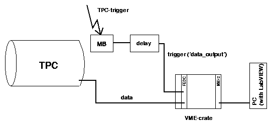
5 Integration in existing setup
|
|
6 Problems
In the CERES version of the ALTRO chip, the zero suppression scheme does not guarantee that the formatted pad data block is smaller than 256 bytes, which is the largest number of bytes that can be stored, for each pad, in the data memory. In this case the bytes in excess will overwrite part of the 256 bytes starting from the first byte in the packet. However, BLENGTH (9 bit word) still should have the correct value.
Footnotes:
1Front End Digitaziation Card
2ALice TPC ReadOut. For the CERES readout a modified version of this chip was used.
3Multisystem eXtension Interface
4VME
eXtensions for Instrumentation