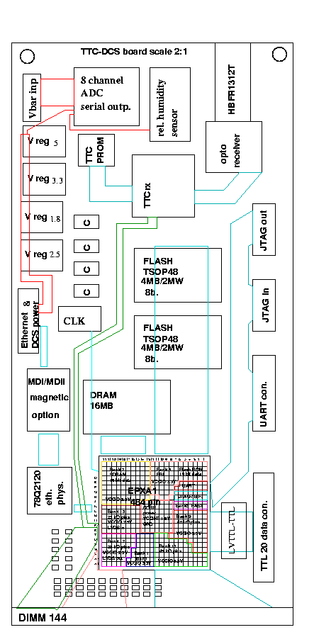
TTC-DCS board
component layout
( original
link by vp)
Following the guidelines outlined last week,
we have tried to outline the board layout . We have encountered several
problems and we made several observations:
-
The smallest ARM based FPGA (EPXA1) supports
LVDS I/O only using an external resistor network (1 resistor/input, 3 resistors/otput
pair) and 2.5 V VCCIO on banks dedicated to LVDS (I/O
Standard SSTL-2 Class II). Only the larger member of EPXA family (EPXA4)
has 16 dedicated LVDS inputs and 16 outputs. They are placed at the edge
rows of the 672 pin package (Bank 3 and 7). So that we'd need one more
voltage reg.
-
484 pin package of EPXA requires routing through
at least 7 rows of pins. Ground and core VCCINT are connected near the
center of chip and it seems, that each of them requires separate layer.
We have not found any guidance concerning the recommended routing on FPGA.
It is therefore difficult to estimate number of layers needed on PCB. It
seems, that >=6 layers would be needed.
-
672 pin package allows better organisation of I/O
pins, they can be slightly closer to the outer edge. But the change of
routing depth is ~10%, so that we have to route instead of 7 rows through
~6. Package is larger 26x26, compare to 22x22 mm of 484 pin package.
-
Out of 161 free I/O pins requires design ~125, out
of them 10 LVDS input pairs and 10 LVDS output pairs. We have to use 33+10+1
resistors of LVDS network.
Here is the preliminary component layout.
It is difficult to estimate free space between chips necessary for routing,
but it should be just first estimate. Estimated board size is 6.4x13.1
cm
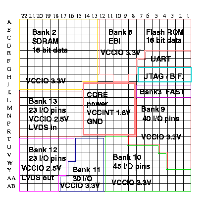
Detail of FPGA package gives better overview of
location of different banks and what they are used for (EPXA1 in 484 Pin
FBGA).
-
2 x 4MB Flash ROM (eg. AMD AM29DL32xD)and standard 16MB SDRAM (eg. Micron
or Infineon) are assumed.
-
Connection of 20 bit data bus requires conversion TTL<->LVTTL!!
-
According to specification of TTCrx asic it can run on 3.3V
-
we have reserved also space for MDI/MDII transformer even when it is nit
forseen to use it. Alternatively this space can be used for OPTO rx/tx
if we'll use such option.
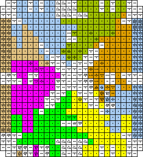
Here is exact distribution of I/O pins to banks and pinouts for
484 pin EPXA1 and APEX20KE400 nios FPGA, where is PLA identical to EXPA4.
Click on them to get full size figure.
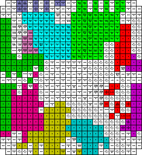 ...
... 
EXPA1
APEX20KE400
It is a question how will the design fit in EXPA1 with (max)
100 K gates, EXPA4 would be on safe side, increase in package size would
be partly compensated since in this case we'd not need resistors for LVDS.
Since in one case are banks selected for LVDS pins concentrated in lower
left corner in the other case APEX20KE400 and probably also EXPA4 is
LVDS I/O placed on left (input) and right (output) side of package.
This would require different routing of LVDS to the DIMM connector.
List of Components:
Power consideration
Power estimation especially of EPXA1 is only rough. There is a white
paper describing how to calculate power consumption in the embedded
stripe, but it focuses on EPXA4 and EPXA10 devices. The other point is
the power consumption of the PLD part and the connection to the PLD part
of the device. Due to the fact, that the hardware design is not finished
power consume can just be predicted.
-
EPXA1: 0.5A..1.5A
-
Ethernet PHY-layer: max. 115mA
-
SDRAM: max. 165mA (@133MHz) Refresh Peak: 330mA
-
Flash ROM: 2x12mA (max. 2x100mA while writing)
-
ADC: 5mA
This makes a possible maximum consumption of more than 2
Ampere.
Board Design
There is an application note from altera (Designing
with FineLine BGA Packages) describing how to place vias and route
out from FBGA. Also some consideration about number of layers are made.
So we should decide which FPGA should be used
from that follows ......==> what will be the LVDS
routing
...............................................======> then we can
fix DIMM connector pinout
!! We still have to think about recovery option when FLASH rom content
is corrupt
16.6.02 V.P. + T.K.