Use of JTAG for reprogramming after Flash ROM failure
For
revitalization of DCS systems where data in the flash boot ROM was destroyed,
a special
JTAG chain should be implemented
to ensure that the system can repair itself by taking data from
a consistent DCS board.
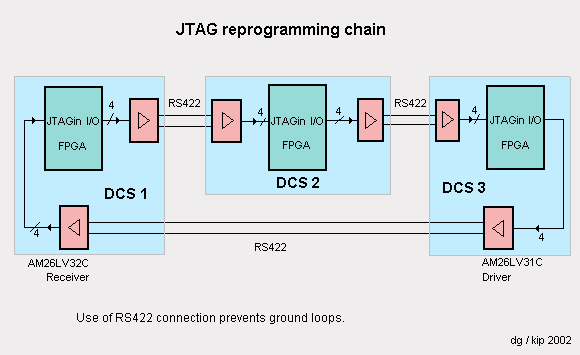
The
picture below shows an example of a chain solution for reprogramming
inconsistent flash data.
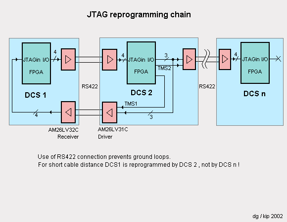
A
compact connector should be used for JTAG interconnection of the
DCS boards.
It will contain four differential
JTAG lines ( DATA, TMS, TRST, TCLK ), driven by RS422
devices for ground loop prevention.
AM26LV31C
with 4 line drivers and AM26LV32C
with 4 line receivers where chosen because of
their 3,3
Volt capability.
A high 15kV ESD
protected, significant lower supply current, TSSOP receiver
device is offered
by MAXIM : the MAX3094E , which
is slightly more expensive ( 1,23$ / 1k / 2002.10.28 )
It should be
considered that the RS422 receivers must still work even if the
FPGA on a DCS fails!
The JTAG outputs of the
FPGA are general user I/Os which emulate a JTAG master when
reprogramming a failed DCS board.