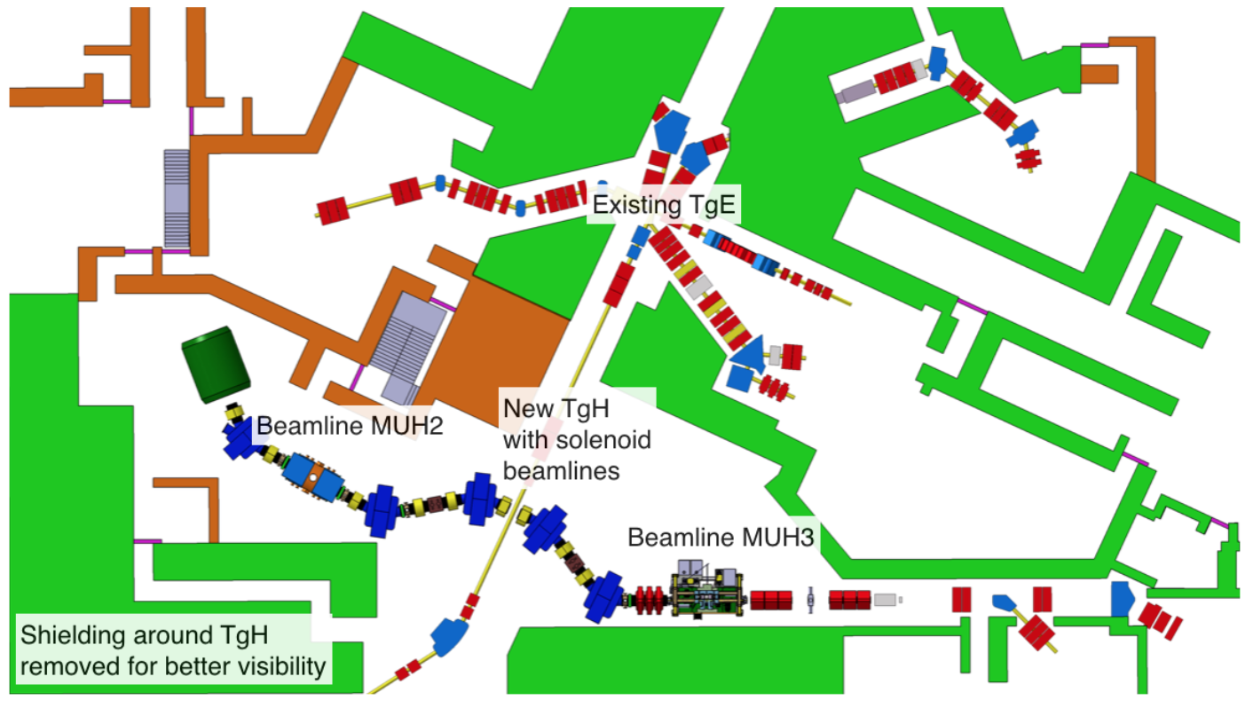
The high muon rate from the HIMB, on the one hand, is necessary for achieving the high sensitivity goal of 10-16. On the other hand, it brings certain challenges; for example, the accidental background events that can mimic our mu3e signal are expected to increase by more than 400 times compared to Phase 1. Suppression of the background levels similar to that of Phase 1 will require modifications to the existing detector design including the muon-stopping target. The Heidelberg mu3e group is involved in R&D efforts to surpass such challenges by employing a detailed Geant4 simulation for the Phase 2 experiment.
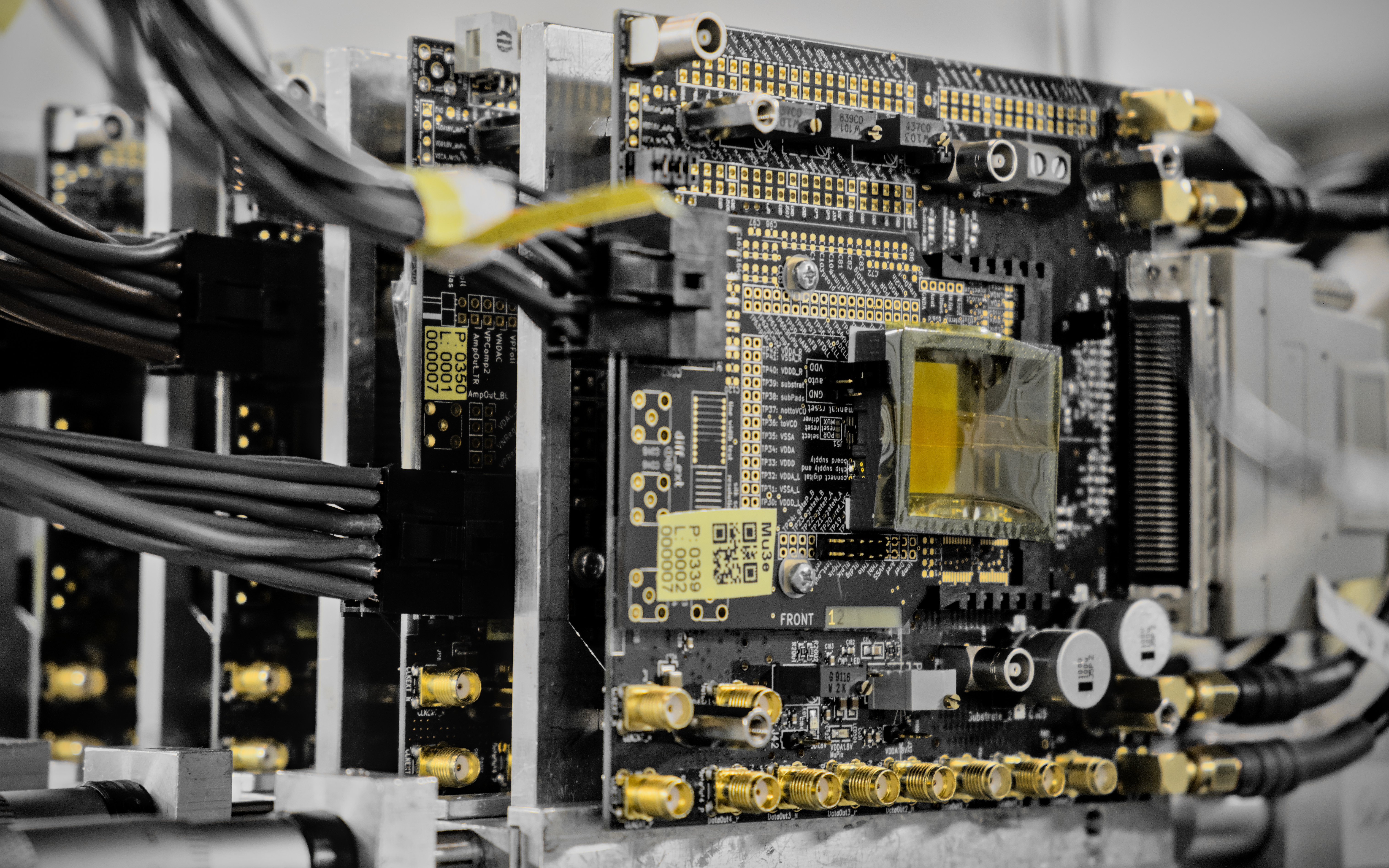
The communication with the chip is handled by the Data Acquisition System (DAQ). The Heidelberg group has developed its own DAQ, which has been used to obtain crucial data in the last years. It consists of several custom cards designed for handling the data connections in and out of the chips, and a FPGA card with a custom firmware. In the effort of developing a more flexible DAQ, new cards are being designed which will communicate with the Mu3e FPGA boards. These provide several fast signal lines and data processing capabilities which can be exploited for more applications.
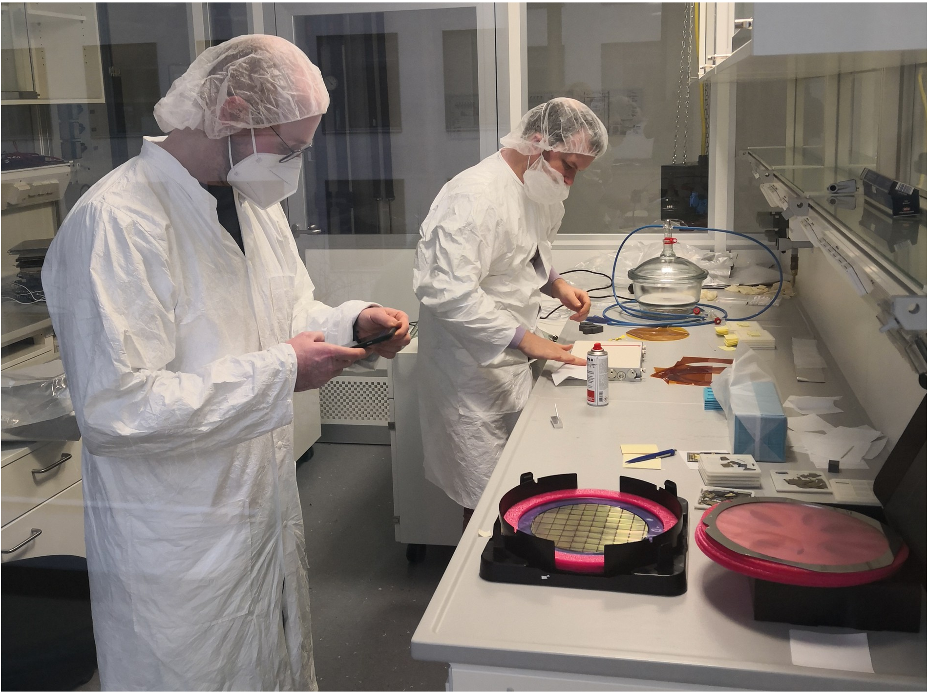
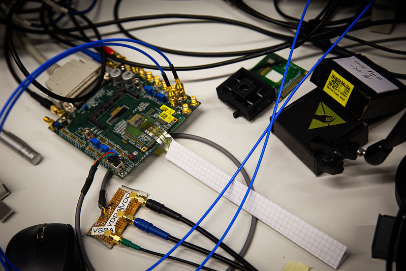
Lab tests are an important step towards the full characterization of a chip. Many of the chip's feature can be studied and understood with the help of several tools, such as oscilloscopes, pulse generators, radiation sources and so on. The Mu3e Heidelberg group has its own lab in the Physics Institute that can host multiple lab setups for chip characterization. The group makes use also of a neighbouring clean room, where several prototypes are assembled and tested in optimal conditions.
The characterization of a chip is not completed without a test beam measurement. In this kind of tests, the devices are brought to a beam line and their response to high energy particles is studied against the particle tracks reconstructed by a telescope. The Heidelberg Mu3e group organizes several test beam campaigns every year, at DESY (Hamburg), MAMI (Mainz) and PSI (Villigen, Switzerland). The group has developed the first telescope based on HV-CMOS pixel detectors and keeps upgrading it to the newest produced prototypes.